GPU 101 for Backend Engineers
How CPUs and GPUs cooperate, how grids, blocks, warps, and tiles execute, and why memory movement matters for LLM inference.
A model can fit in GPU memory and still produce tokens slowly. Increasing the batch size can improve throughput without changing the model or adding hardware. Both behaviors make more sense once we look at how the GPU receives work, distributes it, and moves the data that work needs.
This post builds that execution model for backend engineers. It follows the path from CPU orchestration to GPU hardware, then through blocks, warps, tile programming, and memory. A worked Transformer projection connects those pieces to inference performance.
The examples use NVIDIA CUDA terminology and an illustrative eight-GPU H100 SXM node. Numerical calculations are analytical examples, not measured performance results.
The CPU asks; the GPU executes
The CPU and GPU have different jobs in an inference server. The CPU handles varied, branching work: the API, tokenization, scheduling, and runtime orchestration. The GPU handles large arrays of similar numerical operations.
In NVIDIA’s CUDA programming model, the CPU is the host and the GPU is the device. Each has attached memory. Before numerical work can run efficiently, its inputs and weights must be accessible to the GPU.
A CUDA application starts on the CPU. Host code allocates memory, moves data between processors, launches device work, and waits for completion when a dependency requires it. CPU and GPU work can overlap: while the GPU executes one batch, the host may prepare another. Efficient serving depends on both processors making useful progress.
CUDA is NVIDIA’s platform and programming model for launching computation on its GPUs. A kernel is a device program invoked by the host. One launch starts many lightweight GPU threads, organized into groups, that apply the program to different data. A model runtime normally invokes many kernels per forward pass: matrix operations, normalization, attention, elementwise work, and sometimes communication. The CPU may enqueue work asynchronously, so a host function returning does not necessarily mean the GPU has finished. CUDA streams express ordered device work and allow permitted overlap.
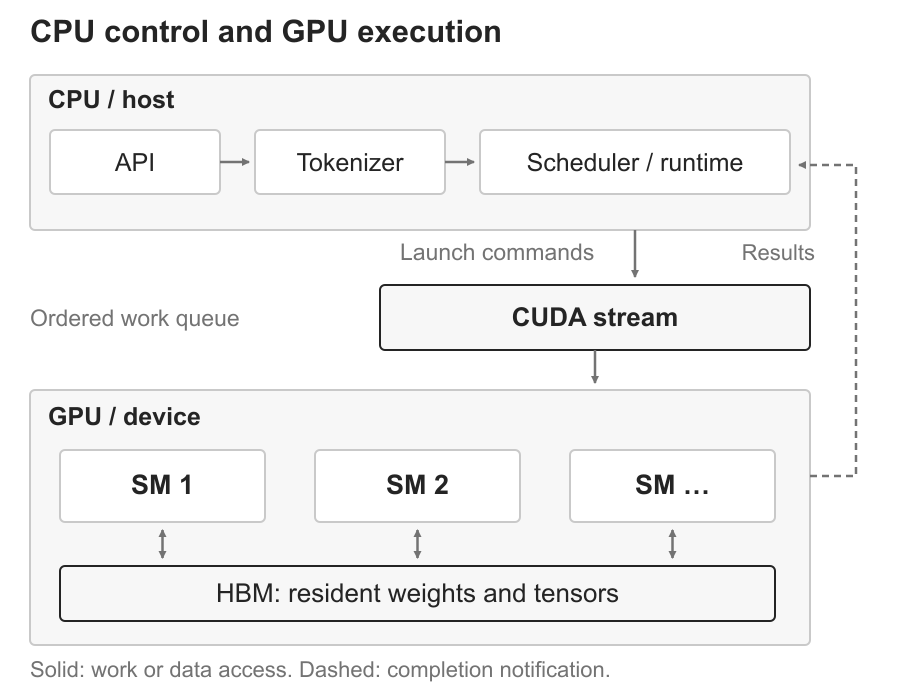
Figure 1. The host supplies commands; kernels execute against device-resident tensors. The diagram is conceptual.
Overlap is useful only when dependencies allow it. If the host needs a token choice before it can schedule the next step, the GPU may wait between kernels. If a required tensor is still in host memory, transferring it adds another delay. Keeping repeatedly used weights resident in GPU memory avoids paying that transfer cost for every token.
A launch returning is therefore different from device work completing. A CUDA stream expresses ordered work; independent streams can overlap when resources and dependencies permit. Adding streams alone does not guarantee more parallel execution.
What is inside the GPU?
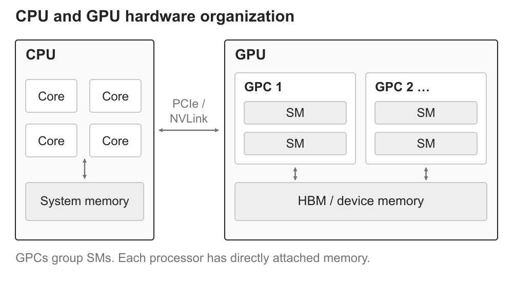
Figure 2. The GPU contains groups of SMs called graphics processing clusters (GPCs), connected to device memory. The CPU has its own cores and attached system memory. The processors communicate through an interconnect such as PCIe or, on suitable platforms, NVLink. Diagram based on the NVIDIA CUDA Programming Guide.
A GPU contains many streaming multiprocessors, or SMs, grouped into graphics processing clusters. An SM combines thread scheduling, arithmetic units, registers, and shared-memory/L1 resources. It is closer to a small execution cluster than to one CPU core or one operating-system worker. NVIDIA describes these components in its hardware model.
CUDA cores perform general arithmetic within an SM. Tensor Cores specialize in supported matrix multiply-accumulate operations. Using them requires suitable kernels, data types, and shapes; arbitrary device code does not automatically gain their advertised throughput. The CUDA tile documentation describes how supported tile operations map to that hardware.
1
2
3
4
Kernel launch: one grid
  └─ Many thread blocks → scheduled onto available SMs
       └─ Warps of 32 threads
            └─ Arithmetic and supported Tensor Core operations
The runtime must expose enough independent work to keep those units useful. A small operation may leave many SMs idle. A larger one can occupy the device and still wait on data. Core counts describe available hardware; the operation’s shape and data movement determine how much of it can help.
Thread Blocks and Grids
A kernel launch can create a very large number of logical threads, sometimes millions. The threads are grouped into thread blocks, and the blocks form a grid. Within a conventional SIMT launch, blocks have the same dimensions. The launch describes the work to perform; it does not mean all of those threads execute simultaneously.
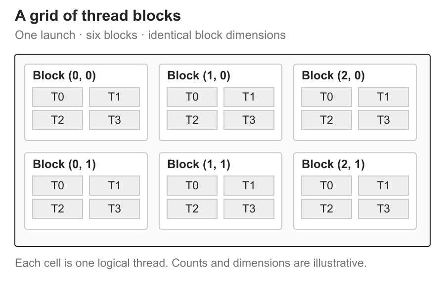
Figure 3. A grid of thread blocks. Each cell represents a logical thread; the thread count is illustrative. Source: NVIDIA CUDA Programming Guide.
Blocks and grids can be one-, two-, or three-dimensional. A launch configuration specifies their dimensions, letting the program map threads naturally to a vector, matrix, or volume. All blocks in a conventional SIMT grid use the same block dimensions.
Each thread can inspect built-in indices to determine which data it owns. In CUDA C++, threadIdx identifies its position in the block, blockIdx identifies the block’s position in the grid, and blockDim and gridDim expose their dimensions. For a one-dimensional launch, a common mapping is:
1
2
3
4
int i = blockIdx.x * blockDim.x + threadIdx.x;
if (i < n) {
    output[i] = input[i] * scale;
}
Here the program maps one logical thread to one array element. A two-dimensional arrangement can instead map threads to matrix rows and columns. These dimensions describe a convenient indexing scheme; the physical SMs are not arranged into that same grid.
A block is assigned to one SM. Its threads can exchange data through shared memory and coordinate with block-level synchronization. That local cooperation is useful for operations that load a small region of data and reuse it together.
A grid may contain far more blocks than the device can keep resident. Available SMs execute blocks in successive waves. A block is assigned to one SM and normally completes there; specialized features such as CUDA dynamic parallelism have exceptions. The device therefore does not need one physical execution cluster per logical block.
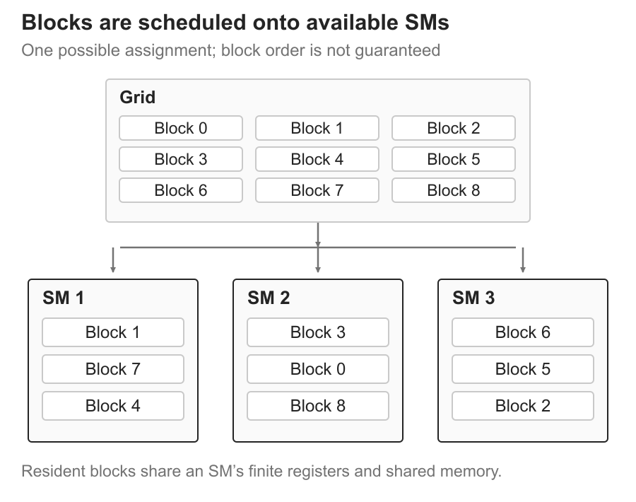
Figure 4. Several blocks can be resident on one SM at once; the pictured example uses three. The order in which blocks reach SMs is not guaranteed. Source: NVIDIA CUDA Programming Guide.
Warps and SIMT
Within a block, threads form warps of 32. A block with 256 threads contains eight warps. A warp is a hardware execution group, not a process.
CUDA’s single-instruction, multiple-thread (SIMT) model lets those threads run the same kernel on different data. They share a program, but they can take different branches. When only some lanes need an instruction, the other lanes are masked during that work.
The block boundary also makes the execution model scalable. An ordinary grid must work whether blocks execute together, in a different order, or in successive waves. A block cannot assume another block has already produced a value or will be scheduled while it waits. Specialized cooperative features provide additional coordination, but ordinary cross-block waiting is not a safe default.
Threads in a block share an SM; their warps need not issue instructions simultaneously. This distinction separates being resident on the device from actively executing an instruction.
For example, if (threadIdx.x % 2 == 0) selects the even-indexed lanes. Those lanes execute the branch body; the odd-indexed lanes do no useful work for those instructions. Figure 5 shows the active mask for one warp.
This is warp divergence. Similar control flow across lanes usually improves useful work per instruction, but the cost depends on the branch and the surrounding kernel. A masked branch does not imply that the entire request loses half its throughput.
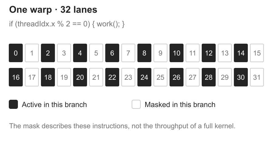
Figure 5. Even-indexed threads execute the conditional body while the other lanes are masked. This illustrates one branch, not a claim that every divergent kernel loses half its throughput. Source: NVIDIA CUDA Programming Guide.
Tile Programming in CUDA
SIMT code describes what each thread does. Tile programming describes what a block does to a multidimensional collection of values. The programmer chooses tile operations; the compiler maps them to individual threads and hardware resources.
Tile kernels still launch on a grid of blocks. A block uses its grid position to find its region of the data. The programmer specifies the grid dimensions, while the compiler determines the internal thread layout from the tile operations. Figure 6 shows the change in the programmer’s view.
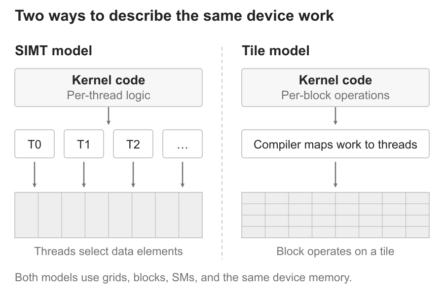
Figure 6. SIMT code expresses work for each thread; tile code expresses operations for a block on multidimensional data. The compiler handles the internal thread mapping. Source: NVIDIA CUDA Programming Guide.
Control flow belongs to the block. Loops and conditionals are supported, but they do not express separate branches for individual lanes. Scalar work, such as calculating an index or loop bound, can be handled by a single thread; tile operations distribute the numerical work across threads. There is no programmer-visible per-lane divergence in this abstraction. The underlying device still executes threads.
Tile operations include elementwise arithmetic, matrix multiplication, reductions such as sum or maximum, reshaping, transposition, and type conversion. For example, a matrix operation can be described conceptually as:
1
2
3
4
5
6
For each output tile:
    initialize accumulators
    for each tile along the reduction dimension:
        load the corresponding tiles of X and W
        accumulate their matrix product
    store the output tile
This is an algorithm sketch, not executable CUDA. One block may operate on multiple tiles: a block groups execution, while a tile groups data. The compiler decides how tile values and operations map to threads and on-chip resources. See Writing Tile Kernels.
Relationship to SIMT programming
The choice is per kernel. An application can mix SIMT and tile kernels, and both can use the same device allocations. SIMT offers direct control over thread behavior, which remains useful for some algorithms and optimizations. Tile programming gives the compiler more responsibility for that mapping.
That responsibility can make a tile kernel portable across supported architectures without manually rewriting its per-thread layout. Portability still depends on toolchain and hardware support. Both models ultimately use SMs, blocks, grids, and the same device memory spaces.
GPU memory
Registers hold values private to a thread, typically the fastest working storage. Shared memory is on an SM and can be used by threads in a block to reuse a tile of data. Global memory is device-wide memory; on our H100 example it is HBM, high-bandwidth memory attached to the GPU. NVIDIA’s CUDA memory-space guide documents the scope and lifetime of these spaces. Cache levels also sit between SMs and HBM. Each memory location trades capacity, speed, and accessibility.
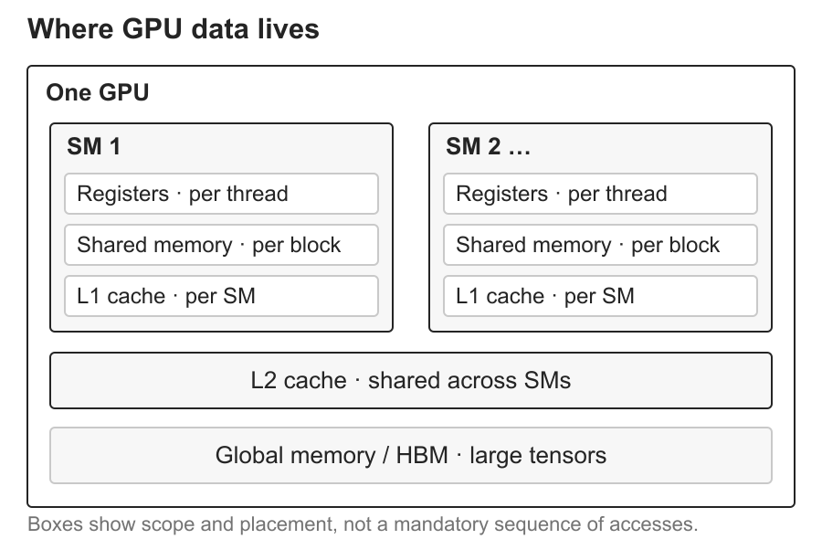
Figure 7. Registers, shared memory, and L1 belong to an SM; L2 and global memory serve the wider device. The nesting shows scope, not an access sequence.
“Slower” here refers to access cost relative to on-chip storage, not a universal latency constant. HBM is extremely fast compared with ordinary storage, yet repeatedly fetching the same weight from HBM can still be the limiting operation in a GPU kernel. The optimization opportunity is to reuse a loaded value for more arithmetic before fetching it again. The analogy to a CPU cache is helpful, but a kernel can explicitly stage data in shared memory and its performance depends heavily on the access layout. The CUDA Best Practices Guide treats memory access and data transfers as central performance concerns.
Each SM has a register file and shared memory. The compiler typically places thread-local working values in registers. Shared memory lets threads in a block exchange and reuse data explicitly. Supported thread-block clusters can also access distributed shared memory with the required synchronization; ordinary blocks do not automatically share each other’s storage.
Registers, shared memory, and occupancy
Registers and shared memory are finite. A kernel that uses more of them per block may run fewer blocks on each SM at once. This is one meaning of occupancy: how much of the SM’s possible resident thread/warp capacity is active under a kernel’s resource limits. More occupancy can help hide stalls, but maximizing it is not the goal by itself; a kernel can do more useful work with lower occupancy if its data reuse is better. NVIDIA’s advanced kernel programming guide explains how register and shared-memory usage limit resident blocks and warps.
Virtual addressing and explicit data movement
Like CPUs, GPUs use virtual memory addressing. On CUDA systems with unified virtual addressing, CPU and GPU allocations occupy a common virtual address space with distinguishable ranges. This lets the runtime identify where an allocation resides, including which GPU owns it. It does not make every pointer directly accessible by every processor, nor does it make physically remote memory as fast as local memory.
CUDA provides APIs for allocating host and device memory, copying between them, and transferring data within or between GPUs when supported. These operations make placement an explicit part of the program. A model loaded into GPU memory at startup need not be copied back from CPU memory for each token.
L1 and L2 caches
Caches complement explicitly managed storage. L1 sits close to an SM and shares physical resources with shared memory on architectures such as Hopper. L2 is shared across the GPU’s SMs. Cache hits can reduce traffic to HBM, but available cache capacity is much smaller than a large model’s full weight set.
Unified memory
In the usual explicit-allocation model, device kernels use device allocations and host code uses host allocations. The program copies data when the consuming processor needs a local copy. There are exceptions, including mapped host memory and platform-specific coherent access, so accessibility depends on allocation type and hardware; a shared virtual address alone is not enough.
Unified Memory allows managed allocations to be accessed by the CPU and GPU. The runtime or hardware arranges access or moves the data as needed. This simplifies the programming interface, but does not remove the physical cost of accessing remote memory or migrating pages.
Placement still matters. Data repeatedly used by the GPU benefits from staying near it. Unified virtual addressing identifies allocations in a common address space; Unified Memory manages shared access. They solve related but different problems.
Why matrix multiplication fits a GPU
Suppose a Transformer layer applies a weight matrix W of shape [8192, 8192] to B token vectors. Arrange the inputs as X with shape [B, 8192]. The result Y = XW has shape [B, 8192]. Each output element sums products of input and weight values. Different output tiles can be calculated in parallel, while each tile can reuse data loaded from HBM. That combination of many independent tiles and local reuse suits the GPU.
Here is the scale of one BF16 weight matrix, with BF16 = 2 bytes per stored value:
1
2
3
4
5
W bytes = rows × columns × bytes/value
        = 8,192 × 8,192 × 2 bytes
        = 134,217,728 bytes = 128 MiB

Work for XW ≈ 2 × B × 8,192 × 8,192 floating-point operations
The result is easier to compare as a table. Assume W contributes one complete read in each case:
| Token vectors B | Approximate arithmetic | Weight bytes | Arithmetic per weight byte |
|---|---|---|---|
| 1 | 0.134 GFLOP | 128 MiB | 1 FLOP/byte |
| 128 | 17.2 GFLOP | 128 MiB | 128 FLOPs/byte |
B counts token vectors in the operation, not necessarily HTTP requests. The factor of two counts a multiplication and an addition per term, approximately.
At B = 128, the arithmetic increases 128-fold while the assumed weight read stays fixed. The same loaded values can support more work. That ratio excludes input/output traffic, repeated weight reads, and cache effects, so it is not measured arithmetic intensity or a promised speedup.
This worked example explains a recurring inference pattern. Processing a prompt supplies many token positions to a matrix operation, so weight tiles can be reused across those positions. Decoding one new token for one request supplies far less work per weight tile. Batching decode tokens from multiple requests can restore some reuse, but it also changes memory demand and request latency. The calculation concerns one dense projection, not the cost of all 80 layers or a full response.
The series’ illustrative running node has eight H100 SXM 80 GB GPUs. Each GPU has its own attached memory; model sharding and communication determine how an operation is distributed across them. This is a teaching configuration, not a reported deployment. NVIDIA’s HGX H100 reference lists 3.35 TB/s HBM bandwidth per GPU. That is a hardware specification, not the rate this projection or an LLM server necessarily achieves. Dividing a byte count by 3.35 TB/s would be a theoretical lower bound under strong assumptions, not a predicted wall-clock latency. The next article in the series formalizes compute and bandwidth bounds. Here, the important distinction is that memory capacity determines what can remain resident, while memory bandwidth affects how quickly kernels can fetch it.
Why peak FLOPs do not equal inference speed
A GPU’s advertised floating-point throughput is a ceiling for specific arithmetic and precision modes. An inference request may miss it for several independent reasons:
- Too little parallel work. Small or irregular matrices do not keep enough SMs and Tensor Cores busy.
- Not enough data reuse. Arithmetic units wait while weights or sequence state arrive from HBM.
- Launch and synchronization gaps. The CPU and runtime enqueue many kernels; dependencies can expose gaps between them.
- Transfers and multi-GPU communication. Host/device copies and GPU collectives occupy time outside the arithmetic of a single kernel.
- Queueing. A request may wait before any GPU work starts. GPU execution time is only one component of user-visible latency.
These causes call for different fixes. A kernel optimization does little for a request whose time is mostly queueing. Increasing batch size may improve weight reuse yet worsen time to first token for newly arrived requests. Adding GPUs may help model fit but also add communication. The right question is where the time and bytes actually go.
References
- NVIDIA CUDA Programming Guide: programming model, SIMT kernels and memory spaces, streams, advanced kernel programming, and tile matrix operations.
- NVIDIA CUDA Best Practices Guide for memory movement, timing, and profiling principles.
- NVIDIA HGX H100 hardware specifications for the stated H100 SXM capacity and bandwidth.
Key takeaways
- The CPU handles control and launches GPU kernels; the GPU executes parallel numerical work against device-resident data.
- SMs execute groups of threads. CUDA cores and Tensor Cores do different work; suitable kernels and enough parallel tiles are needed to use the latter.
- Registers and shared memory provide fast local reuse, while HBM supplies much larger tensors. Movement through this hierarchy can dominate arithmetic.
- Peak FLOPs alone cannot predict request latency. Measure kernel execution, launch gaps, memory movement, communication, and queueing.
Mental model
1
2
3
4
5
6
7
8
9
10
11
CPU: schedule and launch
          ↓
CUDA stream: ordered GPU work
          ↓
Kernel work on SMs ← HBM: large tensors
          ↕
Registers and shared memory: local reuse
          ↓
Output tensors → dependent work / host response

User-visible time also includes queueing and transport.